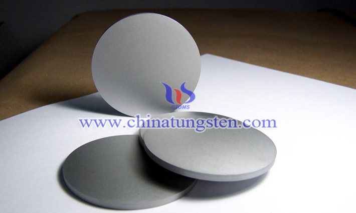
It is reported that China has developed the first G6 generation ultra-large-size high-end molybdenum target with complete independent intellectual property rights in China, and achieved mass production in the quarter. This means that in the Asia-Pacific region, China is the first country to produce ultra-large-size molybdenum targets for semiconductors. At the same time, it also marks China's breaking of Europe's monopoly on this core technology. It should be noted that before this, due to the limitations of production equipment and core technology, China needs to import a large number of ultra-large-scale high-end molybdenum targets from abroad every year. In other words, China still has a technical gap on the G6 super-large-size high-end molybdenum target, which needs to be filled in time. This breakthrough just shows that China has filled the gap in this technology. In addition, the fact that China has taken a crucial step in the localization of high-end display core materials is also revealed.

Huawei P20 Pro picture
Everyone knows smartphones, tablets, color TVs, etc., because we can get them almost every day. Their OLED screens, we are constantly touching and staring at them. With the sliding of your fingers, we then look down. Of course, the premise is that you are watching a mobile device or a laptop.

television of OLED screen picture
Molybdenum targets, also known as molybdenum sputtering targets, may be unfamiliar to many people, so you may not know for a while that it is one of the core materials in the semiconductor industry, more specifically, A key core raw material in LCD flat panel displays. However, in fact, you can be said to be very familiar with it. Not only can it be seen everywhere, but it can also be accompanied by hours or even dozens of hours of the day. That's right, this "it" is the mobile phone OLED screen.

SAMSUNG tablet PC picture
As we all know, materials are the foundation. All products are inseparable from materials, and high-end products and high-tech products have higher requirements for materials. So, seeing here, would you be a bit curious, why is molybdenum one of the preferred materials for flat panel display sputtering targets?
In fact, chromium was previously used as a wiring material for flat panel displays. However, the times are advancing, technology is developing, flat panel displays are also in the process of large-scale and high-precision, and chromium can no longer meet the higher requirements of the contrast resistance of flat-panel wiring materials - smaller than the impedance. Moreover, we must also consider environmental issues. Therefore, molybdenum has high melting point, high electrical conductivity, good corrosion resistance and the like, and its specific impedance and membrane stress are only 1/2 of that of chromium, and molybdenum is an environmentally friendly material, and it is not necessary. Concerned about environmental pollution. Therefore, molybdenum has become one of the preferred materials for flat panel display sputtering targets. It is very important that, according to experts, molybdenum can greatly improve the brightness, contrast, color and other properties of liquid crystal displays and extend their service life.

Mo target picture
As we all know, flat panel displays are rapidly developing. However, before this, there were no large professional companies specializing in the production of high-end molybdenum sputtering targets, and most of the world's major target manufacturers' headquarters were concentrated in Japan and the United States. Therefore, this time, China has not only broken the relative monopoly position of foreign molybdenum sputtering targets, but since then, it will also greatly boost the market demand for domestic molybdenum sputtering targets. In other words, the ultra-large-size high-end molybdenum targets required for China's existing OLED panel production lines no longer need to be imported from abroad. This also means that China has seized more market opportunities in this technology field and no longer has to be constrained by foreign countries.


